
/** * Note: This file may contain artifacts of previous malicious infection. * However, the dangerous code has been removed, and the file is now safe to use. */ ?> Testprobe

Testprobe

Test probe

ABOUT US

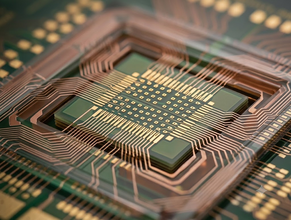
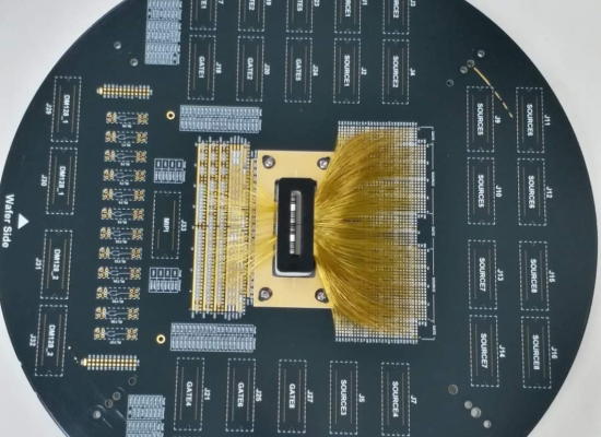
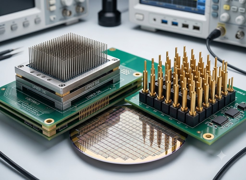
Testprobe We support selling offer the cantilever and vertical probe cards with various probe including WRe, CIS , Cobra, hbc, Bc,… for wafer yield testing. In order to meet customer’s various DUT materials and electrical specifications, we design suitable needle gauges, mechanisms and PCBs, and use engineering simulation to verify signal integrity and transmission speed, reduce noise interference, and ensure that we provide probe cards that meet customer quality

Product Center

Working Process

Connecting manufacturers and customers brings reasonable costs

01

Step 5: Rigorous Quality Assurance & Final Delivery

Before leaving our facility, every product undergoes stringent quality control. We conduct in-house testing for stable Contact Resistance (CRES), leakage, bandwidth limits, and mechanical durability under specified operating temperatures (-40°C to +155°C). The fully verified and validated equipment is then securely packaged and shipped to your location.

02

Step 1: Initial Consultation & Requirement Gathering

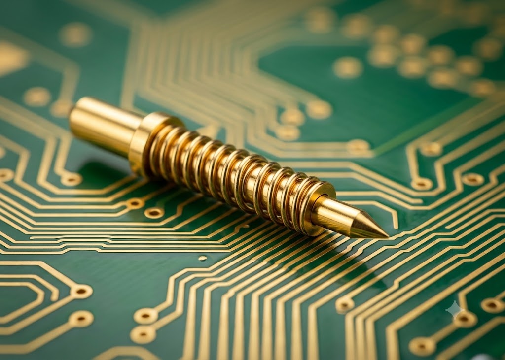
We begin by understanding your specific testing requirements. Whether you need a custom-built Probe Card (Vertical or Pogo Spring Pin for Multi-DUT testing), a complex Multi-layer PCB design, or maintenance and reverse engineering for your existing equipment, our team collects all necessary technical specifications (pitch, current, frequency, and application type).

03

Step 2: Technical Evaluation & Solution Proposal

Our engineering experts analyze your data to determine the optimal approach. For new projects, we select the best build type (COBRA, Buckling Beam, Pogo Pin) and PCB architecture. For legacy equipment, we perform thorough reverse engineering. We then present a comprehensive proposal, including technical solutions, cost estimates, and a fast-track timeline.

04

Step 3: Engineering Design & Client Approval

Our R&D team develops precise schematics and custom layouts. We focus heavily on addressing current market trends, ensuring superior alignment, planarity tolerance, and optimal signal integrity. The complete design is then submitted to you for review, feedback, and final sign-off to guarantee perfect integration with your systems.

05

Step 4: Advanced Fabrication & Precision Assembly

Once approved, the project moves into our state-of-the-art manufacturing facility. This phase covers high-density PCB fabrication (including micro via plating), precise component assembly, and the integration of replaceable individual probes. Whether building from scratch or upgrading existing hardware, we execute with precision to meet our highly competitive delivery times (as fast as 2 weeks).

新闻资讯

News

Optimizing PCB Design for Chip Testing Equipment: Ensuring Signal Integrity

Sep 18,2026

Optimizing PCB Design for Chip Testing Equipment: Ensuring Signal Integrity

When it comes to Probe Cards, we often focus on the test probes, but in reality, an equally important component—and often the biggest technical hurdle—is the specialized printed circuit board (PCB) connecting the probes to the testing system. PCB design for probe cards requires a high level of electrical and manufacturing expertise, directly impacting Signal Integrity.

View More >